(China (Mainland))

Product Summary
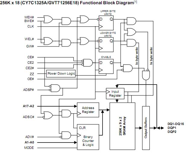
The GVT71256E18T-9 is a 256K x 18 Synchronous Flow-Through Burst SRAM. It employs high-speed, low-power CMOS designs using advanced triple-layer polysilicon, double-layer metal technology. The GVT71256E18T-9 memory cell consists of four transistors and two high-valued resistors. The GVT71256E18T-9 integrates 262,144x18 SRAM cells with advanced synchronous peripheral circuitry and a 2-bit counter for internal burst operation.
Parametrics
GVT71256E18T-9 absolute maximum ratings: (1)Voltage on VCC Supply Relative to VSS:–0.5V to +4.6V; (2)VIN:–0.5V to +VCC+0.5V; (3)Storage Temperature (plastic):–55℃ to +125℃; (4)Junction Temperature:+125℃; (5)Power Dissipation:1.4W; (6)Short Circuit Output Current:100 mA.
Features
GVT71256E18T-9 features: (1)Fast access times: 7.5 and 8 ns; (2)Fast clock speed: 117 and 100 MHz; (3)Provide high-performance 2-1-1-1 access rate; (4)Fast OE access times: 4.0 ns; (5)3.3V –5% and +10% power supply; (6)2.5V or 3.3V I/O supply; (7)5V tolerant inputs except I/Os; (8)Clamp diodes to VSSQ at all inputs and outputs; (9)Common data inputs and data outputs; (10)Byte Write Enable and Global Write control; (11)Three chip enables for depth expansion and address pipeline; (12)Address, data and control registers; (13)Internally self-timed Write Cycle; (14)Burst control pins (interleaved or linear burst sequence); (15)Automatic power-down for portable applications; (16)Low profile 119-lead, 14-mm x 22-mm BGA (Ball Grid Array) and 100-pin TQFP packages.
Diagrams
 |
 GVT71256ZB18 |
Other |
|
Data Sheet |
Negotiable |
|
||||
|
GVT71256T18 |
Other |
|
Data Sheet |
Negotiable |
|
||||
|
GVT71256DA18 |
Other |
|
Data Sheet |
Negotiable |
|
||||
|
GVT71256C36 |
Other |
|
Data Sheet |
Negotiable |
|
||||
|
GVT71256B36 |
Other |
|
Data Sheet |
Negotiable |
|
||||
|
GVT71128ZC36 |
Other |
|
Data Sheet |
Negotiable |
|
||||